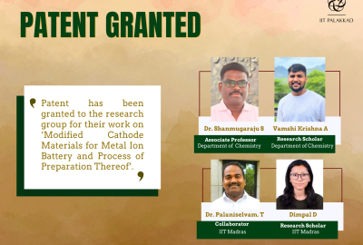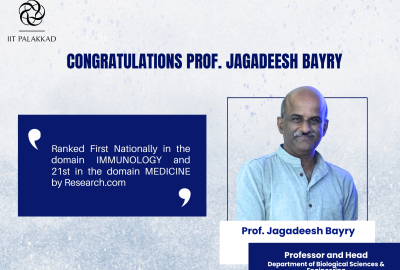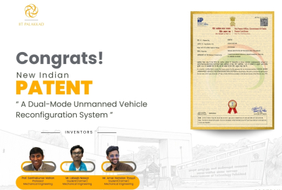
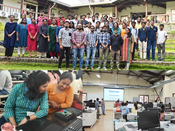
Two-Day Hands-on Workshop on VLSI & FPGA Design Conducted at IIT Palakkad
Department of Electrical Engineering, Indian Institute of Technology Palakkad, in association with the Center for Continuing Education (CCE) conducted a Two-Day Hands-on Workshop on “VLSI & FPGA Design” on 21–22 March 2026 at the Sahyadri Campus under the Mannpower Generation as part of the funded project under the scheme of “Chips to Startups (C2S)” Program, Ministry of Electronics & Information Technology (MeitY). The workshop was co-ordinated by Dr. Subrahmanyam Mula, Associate Professor, Dr. Sabarimalai Manikandan, Associate Professor, research scholars along with UG and PG student volunteers from the Department of Electrical Engineering. 42 students representing 15 institutions from Kerala and Tamil Nadu attended the workshop, demonstrating strong interest and enthusiasm for VLSI design and implementation.
Over the two days, participants engaged in a series of interactive sessions and hands-on learning activities covering key aspects of VLSI Design, including algorithm mapping to efficient VLSI architectures, Verilog for RTL design, ASIC design flow using industry-standard EDA tools, and FPGA prototyping. The practical sessions formed the core of the workshop, enabling participants to gain real-time experience in implementing and analyzing VLSI designs.
The workshop aligns with national initiatives such as the India Semiconductor Mission (ISM) and the C2S Programme, contributing to the development of a skilled and industry-ready semiconductor workforce in India.